Instrumentation for High Frequency electronics
The Instrumentation Circuits area of the PLATINOM platform in the XLIM laboratory provides researchers, academics and industry with access to cutting-edge linear and non-linear metrology measurement tools.
This technical platform comprises a set of equipment and benches for measurements of microwave and sub-millimetric devices allowing the characterization of components, circuits and materials dedicated to applications in the field of telecommunications, space, defence and security.
All these equipments constitute a fundamental element in the research work developed within the various axes and teams of the XLIM Institute.

Instruments and characterization benches available
Material characterization (110 -170 GHz)
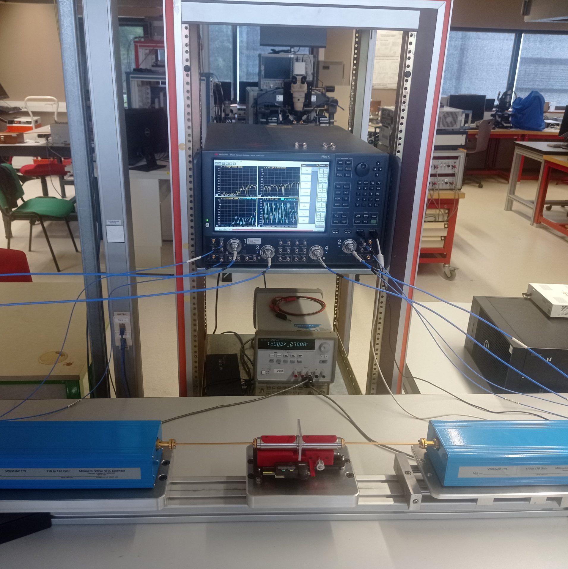
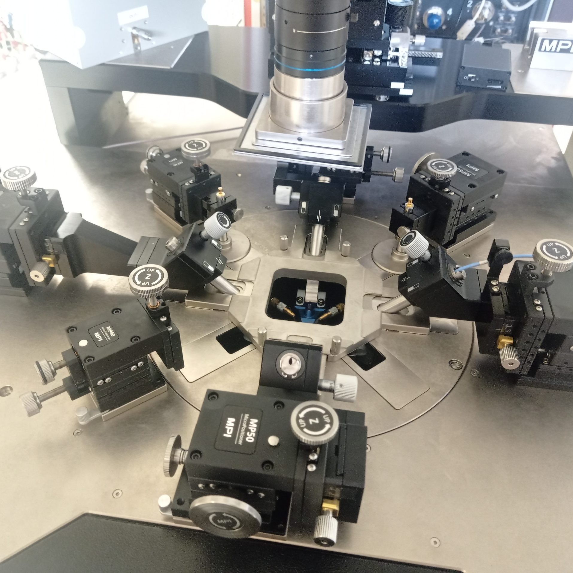
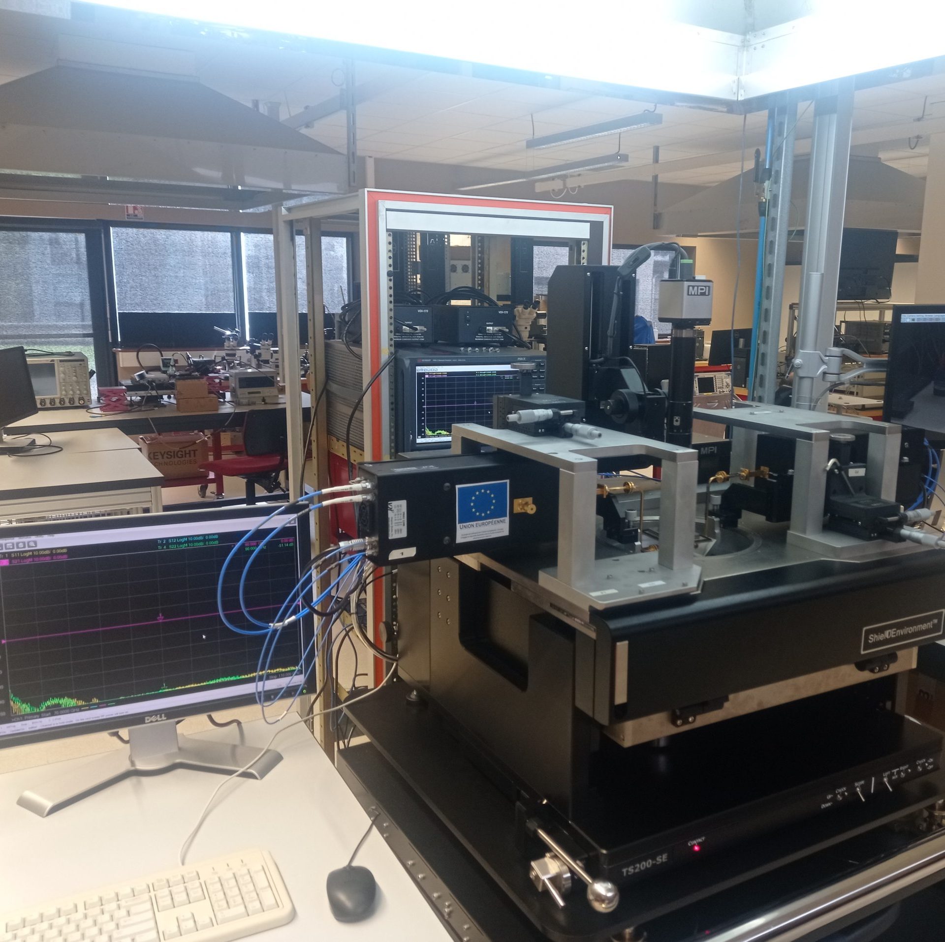
Multiports S parameter characterization
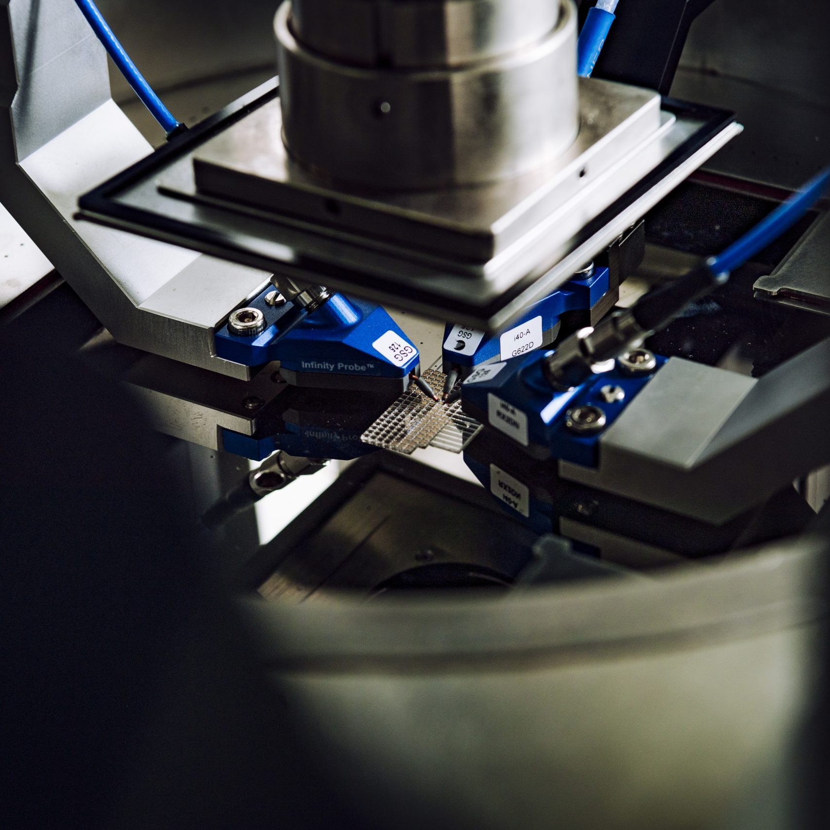
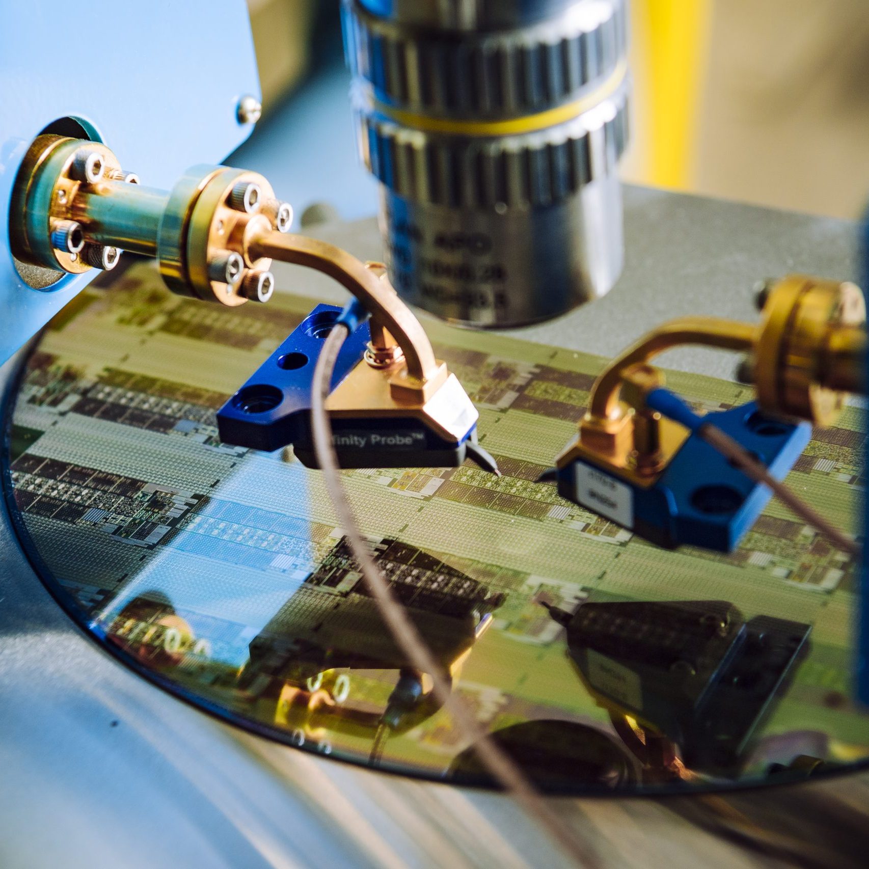
On-wafer devices characterization (S parameters 110-170GHz)
Multiports S parameter characterization bench
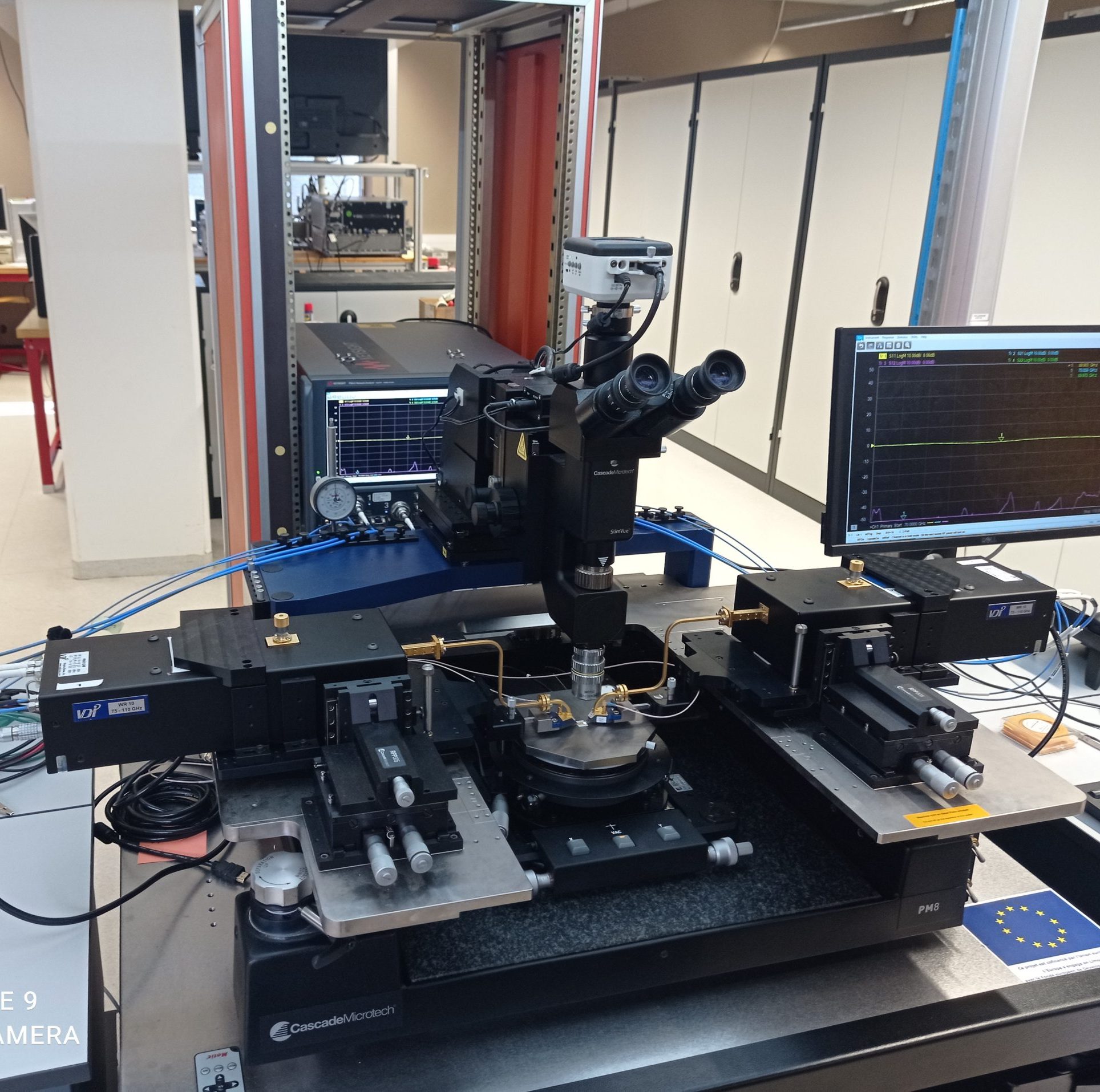
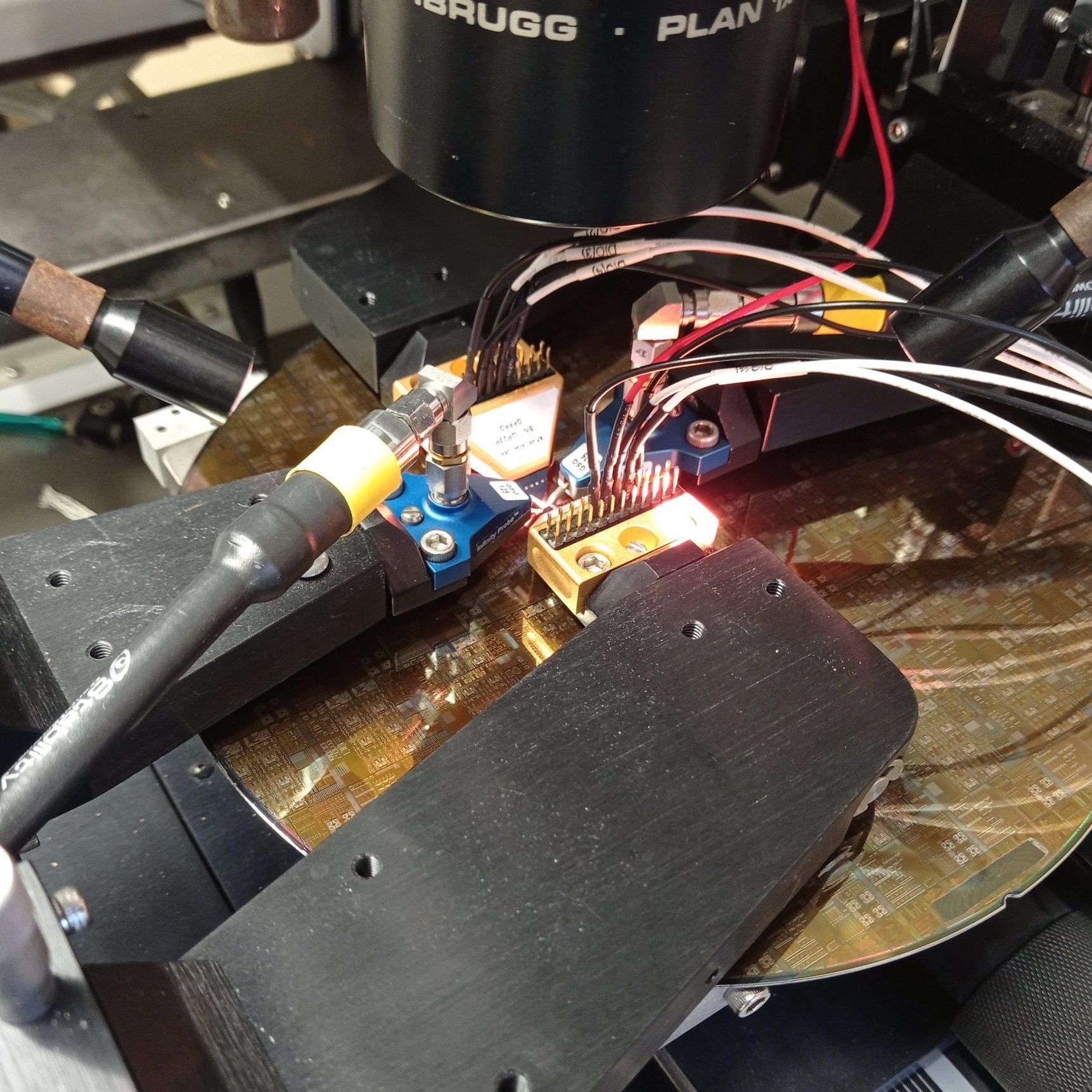
On-wafer devices characterization (S parameters)
On-wafer devices characterization (S parameters)
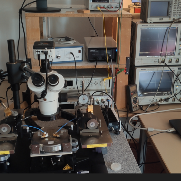
Low Noise amplifier characterization (until 50GHz)
I(Current) / V(Voltage) devices characterization
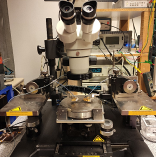
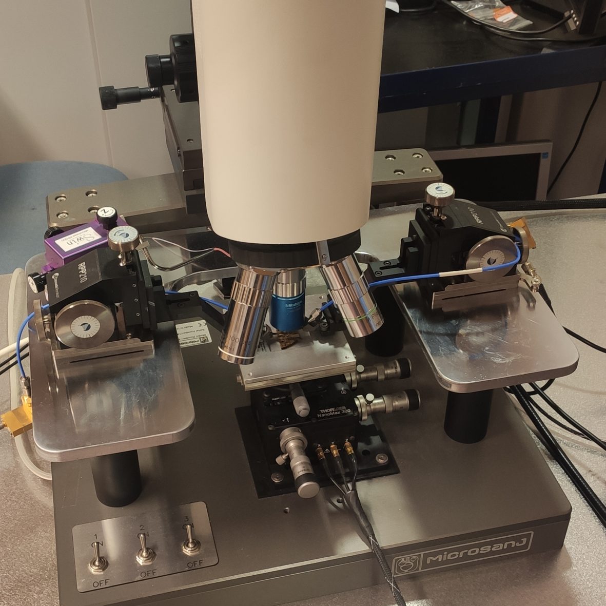
IDLTS bench
Thermoreflectance bench
Services available - contact us
Linear metrology:
– [S] Parameter measurements 10 MHz – 330 GHz
– Noise Factor (NF 50 ohms + parameters [S]) 10 MHz – 50 GHz
Non-linear metrology:
– Frequency/time measurements CW power Load-Pull 1 GHz – 40 GHz (gain, efficiency, harmonics, IMD)
– Frequency/time measurements in modulated signals power (EVM, ACPR, NPR) 1 GHz – 50 GHz
– Impulsive IV Measurements
– IDLTS Measurements
– Thermoreflectance measurements
Material characterization:
– Material characterization up to 330 GHz
Testing and assembly of components:
– Wire Bonding
Ressources
Videos, virtual tour, publications
– Design and Additive Microfabrication of a Two-Pole 287-GHz Waveguide Bandpass Filter IEEE Microwave and Wireless Components Letters, 2020, 30 (1), pp.20-22. https://doi.org/10.1109/LMWC.2019.2955595
– Non-Linear Simulation by Harmonic Balance Techniques of Load Modulated Power Amplifier Driven by Random Modulated Signals, Electronics, 2024, 13 (5), pp.947. https://doi.org/10.3390/electronics13050947
Cliquer sur l’image pour lancer la visite virtuelle du domaine Instrumentation Circuits