GB_Technologie Circuits – Electronique Imprimée
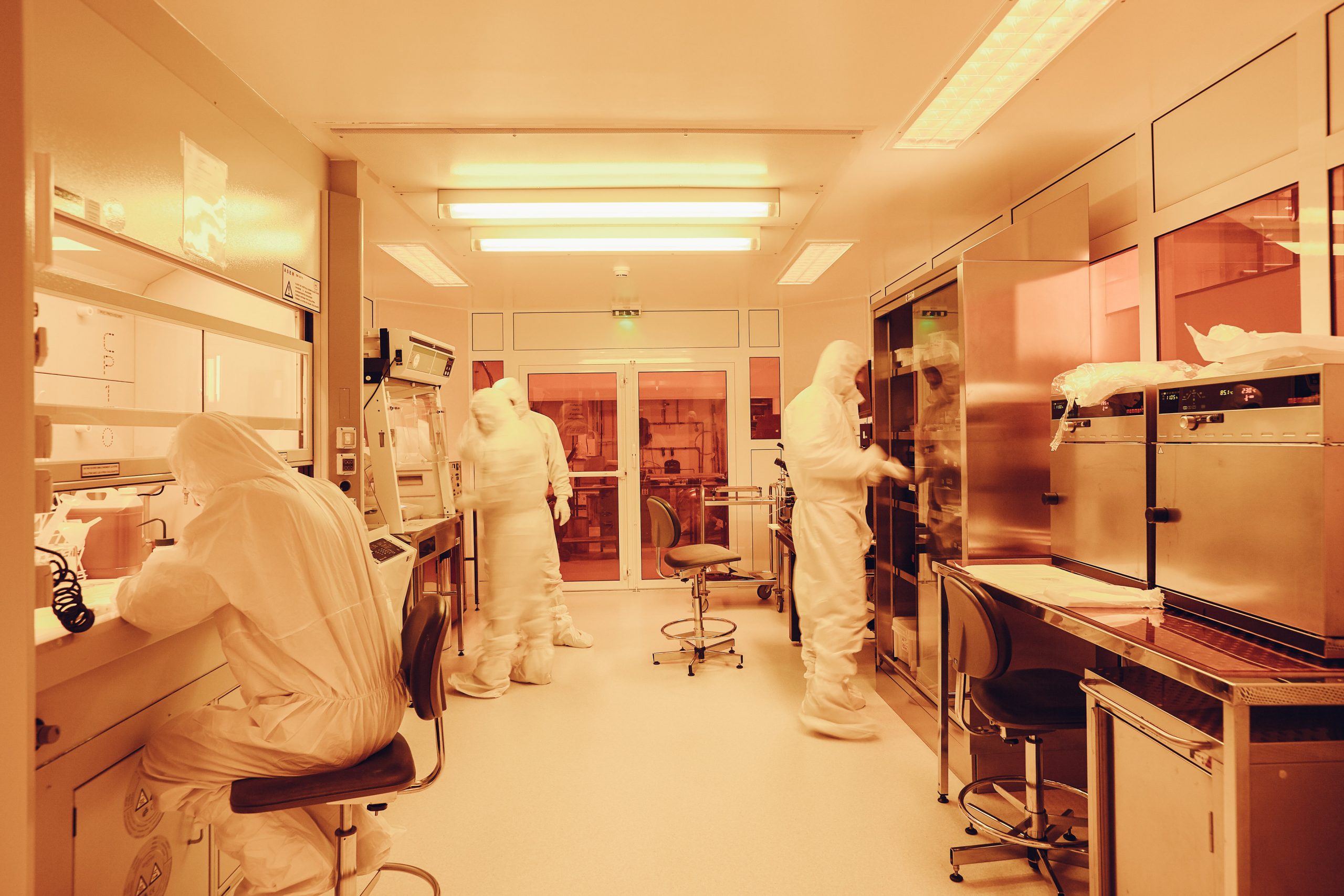
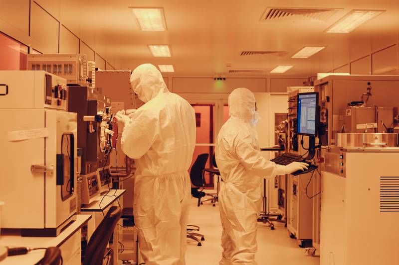
The PLATINOM platform’s Circuits Technology – Printed Electronics domain gathers a range of technological resources for the development of manufacturing processes for silicon and non-silicon Micro and Nanotechnology components and micro-devices (RF MEMS, RF cavities, micro-fluidic circuits, etc. ) covering radio frequency bands up to THz, printable organic optoelectronic devices (photovoltaic cells, field-effect transistors, light-emitting diodes, sensors, etc.) and innovative oxidised materials (PCM, etc.). It also brings together tools for characterising materials and devices using morphological, optical, electrical and optoelectronic techniques. This technology centre covers more than 710 m², including 180 m² of cleanroom area. The domain is a member of the RENATECH + network, a national network of major technology centres. It is also open to the service providers

The PLATINOM platform’s Circuits Technology – Printed Electronics domain gathers a range of technological resources for the development of manufacturing processes for silicon and non-silicon Micro and Nanotechnology components and micro-devices (RF MEMS, RF cavities, micro-fluidic circuits, etc. ) covering radio frequency bands up to THz, printable organic optoelectronic devices (photovoltaic cells, field-effect transistors, light-emitting diodes, sensors, etc.) and innovative oxidised materials (PCM, etc.).
It also brings together tools for characterising materials and devices using morphological, optical, electrical and optoelectronic techniques.
This technology centre covers more than 710 m², including 180 m² of cleanroom area. The domain is a member of the RENATECH + network, a national network of major technology centres. It is also open to service providers.
Micro and Nanotechnologies
UV optical lithography
The micro and nanotechnology centre has two mask aligners (Suss Microtec MJB4 and EVG 610) for UV 365 nm and 405 nm exposure of photosensitive polymers. They enable us to achieve resolutions close to the micron and to develop processes on a wide range of microelectronics resins (S1800, SPR 220-7.0, AZ IPS 6090, AZ 15 nXT, AZ 125 nXT, AZ nLof 2020, DF 50µm and 100µm dry films, etc.). We can align all types of unconventional substrates, sizes and shapes from a few mm² up to 4″.
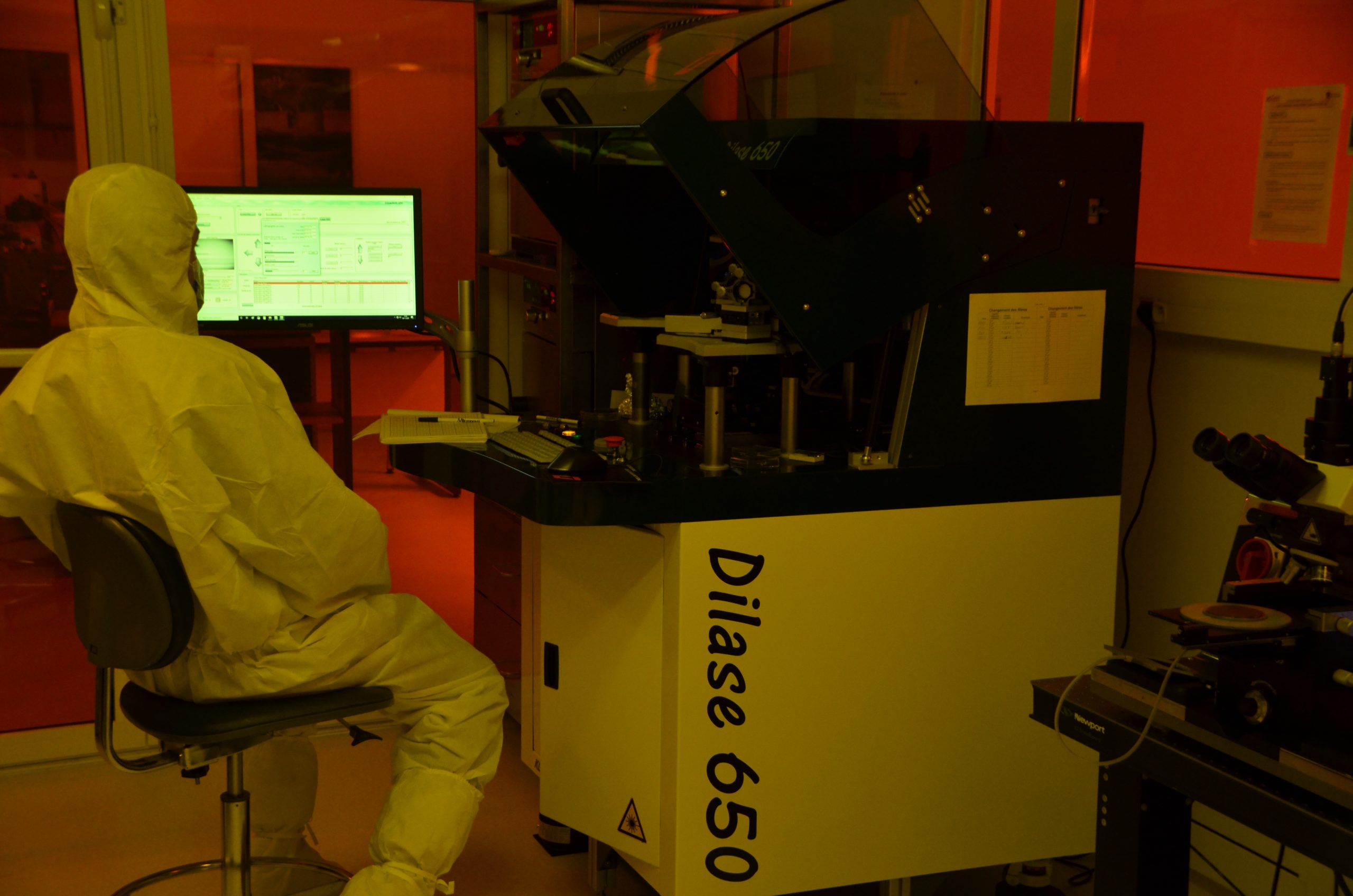
Direct UV laser lithography
In addition to mask aligners, we have a lithography machine using a 375 nm UV laser (Dilase 650 – Kloé), which can write with most of the usual photolithography resins on any type of substrate (glass, flexible, etc.). Writing resolution is just under a micron.
3D additive micro-fabrication
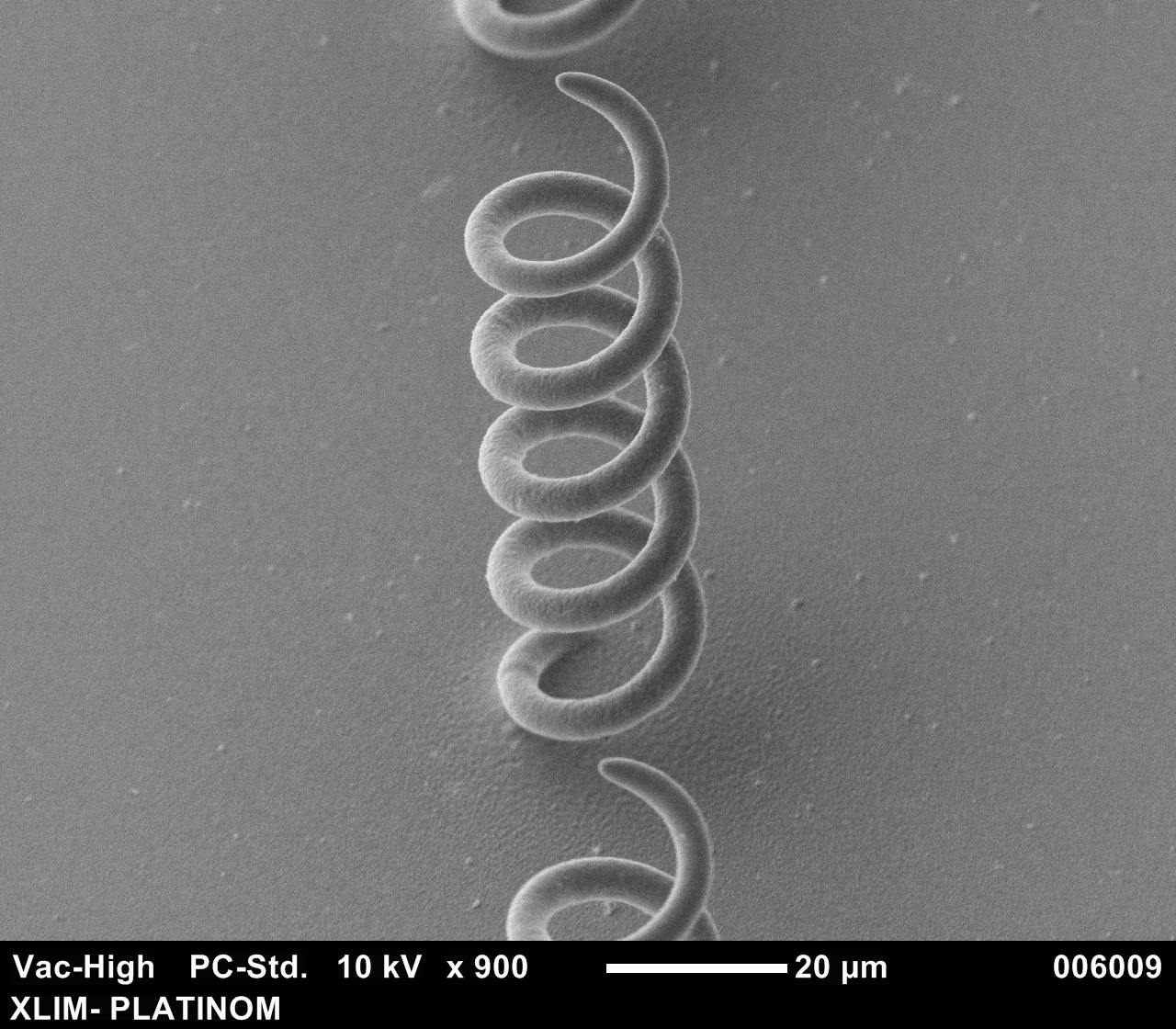
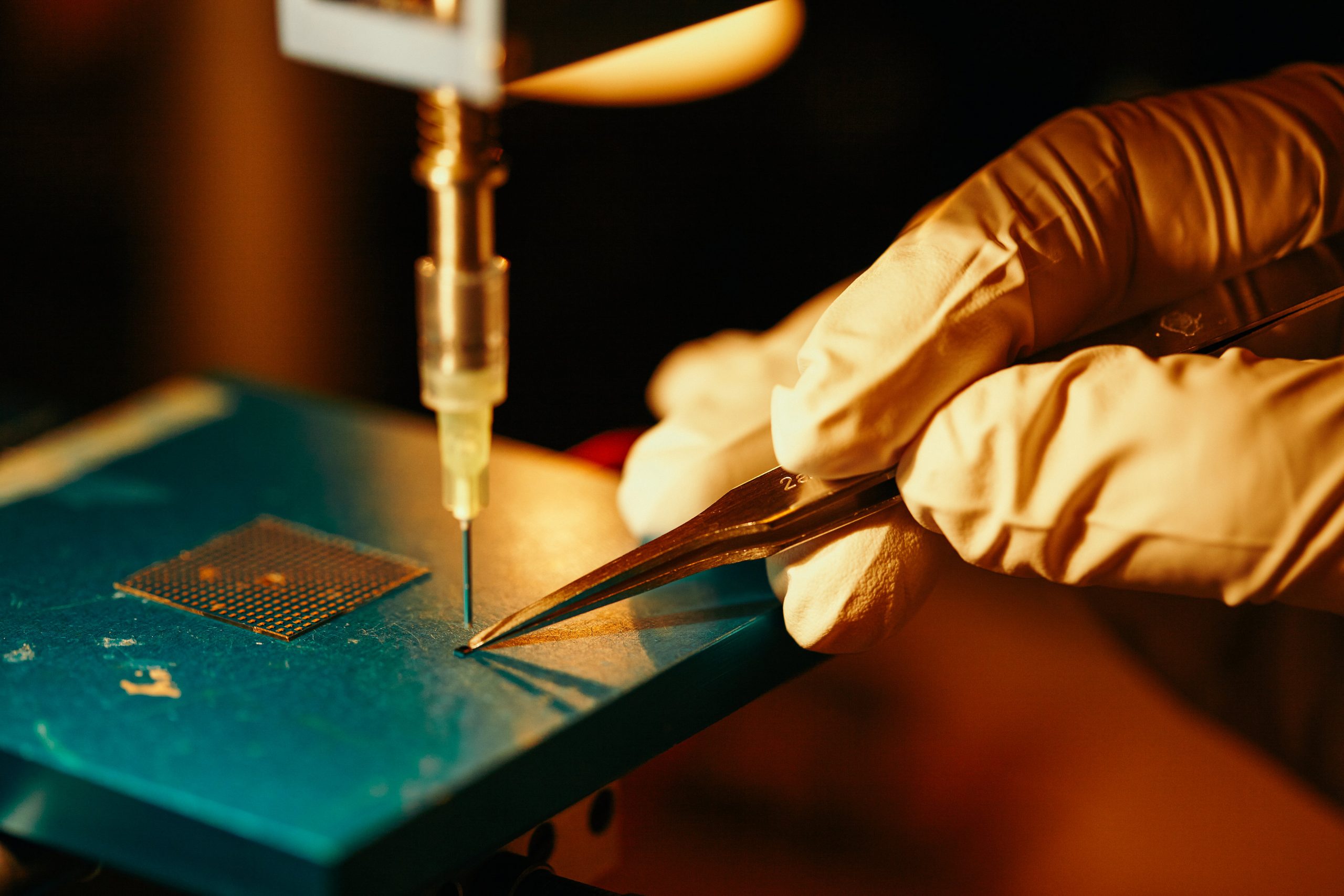
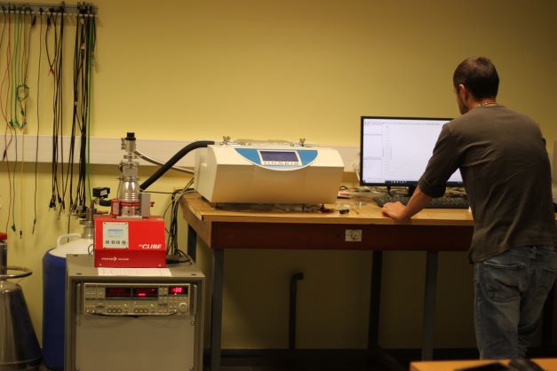
EXADDON’s CERES 3D micro-printing system can print metallic voxels (copper) using an electrochemical process to produce complex micro-structures with micron-level resolution. This equipment is unique in France.

Pure gold and copper electrolytic refills
We have two fume cupboard electrochemistry benches for thickening thin metallic layers of gold and copper. The thicknesses deposited range from a few hundred nanometres to a few tens of microns (pure gold) and a few hundred microns (copper) over a few mm² up to 4″. A third bench is dedicated to the electroless growth of copper layers for 3D objects.
Wet chemical etching
A fume cupboard is dedicated to handling concentrated and diluted acids and bases for wet etching metal layers, oxides and silicon (TMAH, HF, BOE, etc.).
Thin film deposition techniques
The micro and nanotechnology centre also gathers several thin-film deposition techniques covering a wide variety of material properties. We have acquired expertise in a wide range of equipment, including :
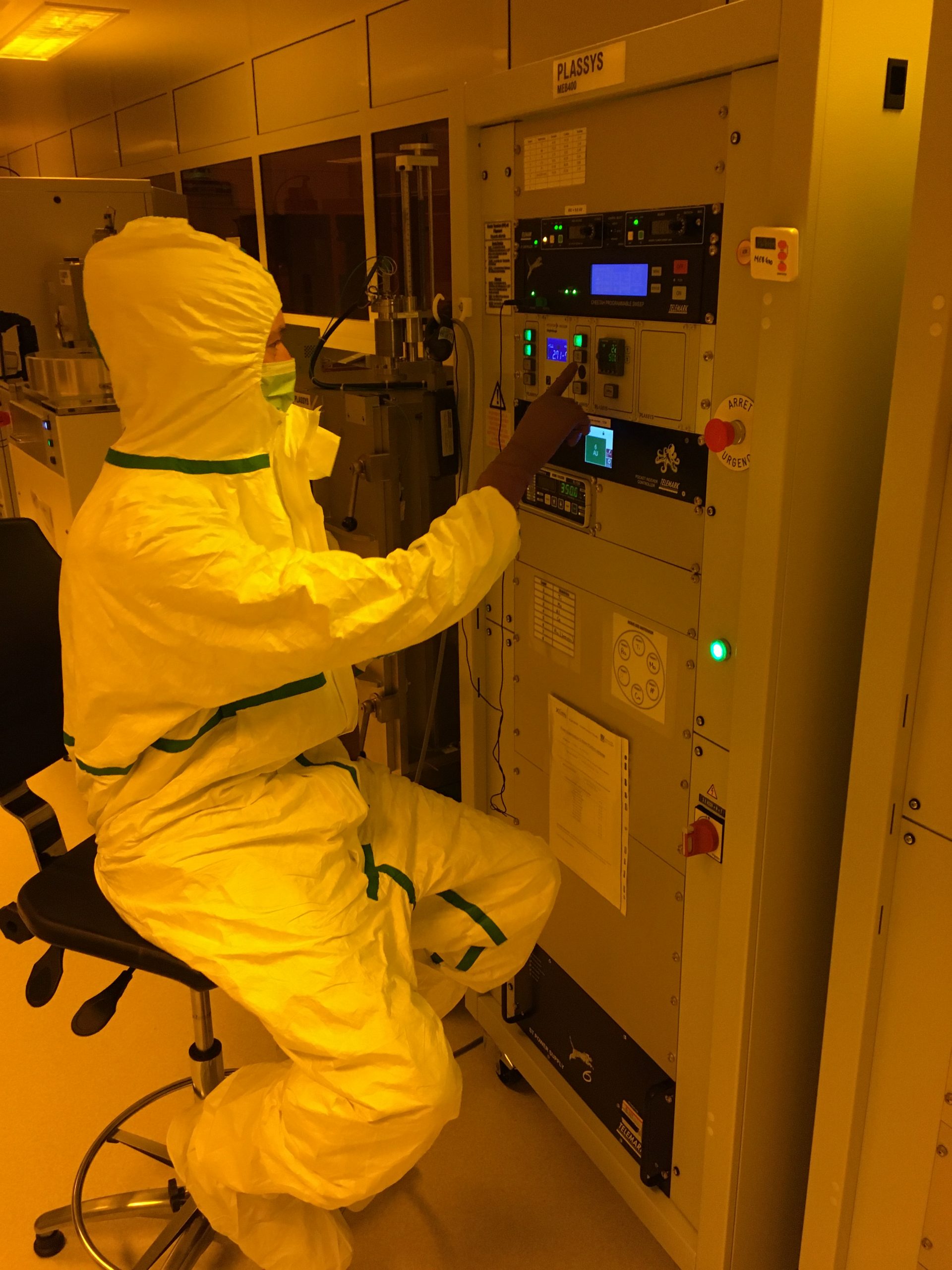
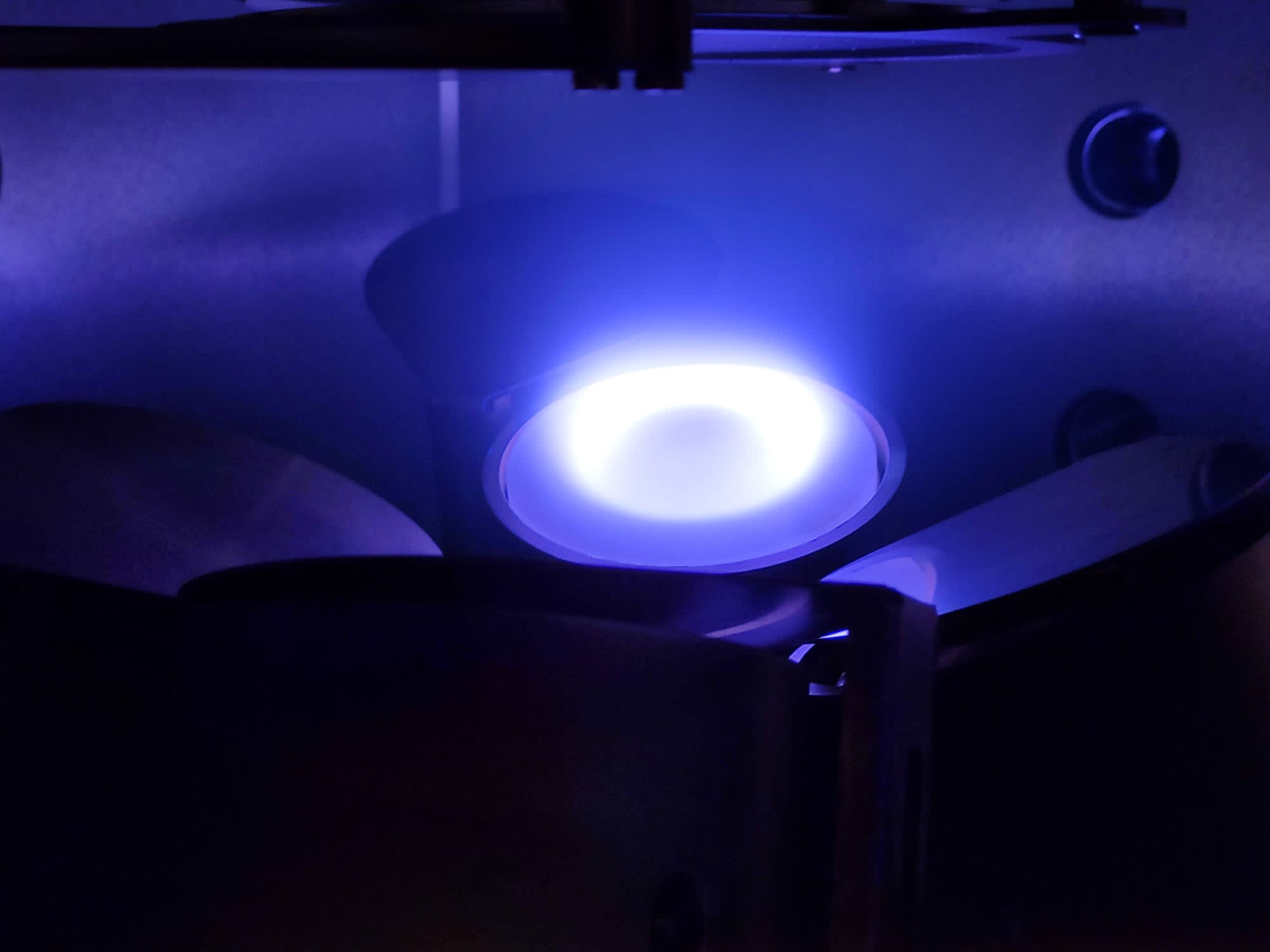
– Two vacuum deposition systems for various metals (Au, Ti, Al, Ni, Cr, Cu, Mo, Pt) using the electron beam evaporation technique (Plassys MEB 300 and MEB 400).
– An electron beam deposition system (Plassys MEB 500) for co-evaporation (Tri-cannons) of metallic or oxide materials (VO2),
– Three DC 2″ and DC 3″ (Plassys MP 300) as well as pulsed DC and RF 3″ (Vinci Technologies PVD6) sputter deposition systems for the deposition of metallic (Al, Ti, Cu, Mo, GeTe, Ti, etc.), nitrided (AlN, TaN, etc.) and oxidised (Al2O3, Ta2O5, SiO2, ZnO, etc.) layers.
– A PECVD (Corial D250) system for the deposition of nitrided thin films (SixNy),
– An eximer laser ablation thin film deposition system (Compex Pro 110 Ne-KrF*) for multilayers and doping (C, Ni, Ag, SiC, GeTe, Al2O3, etc.).
Reactive plasma dry etching processes
We are also equiped with vacuum equipment for the fluoride etching (SF6) of thin metal and nitride layers:
– A Plassys MG 200 RIE plasma etching system,
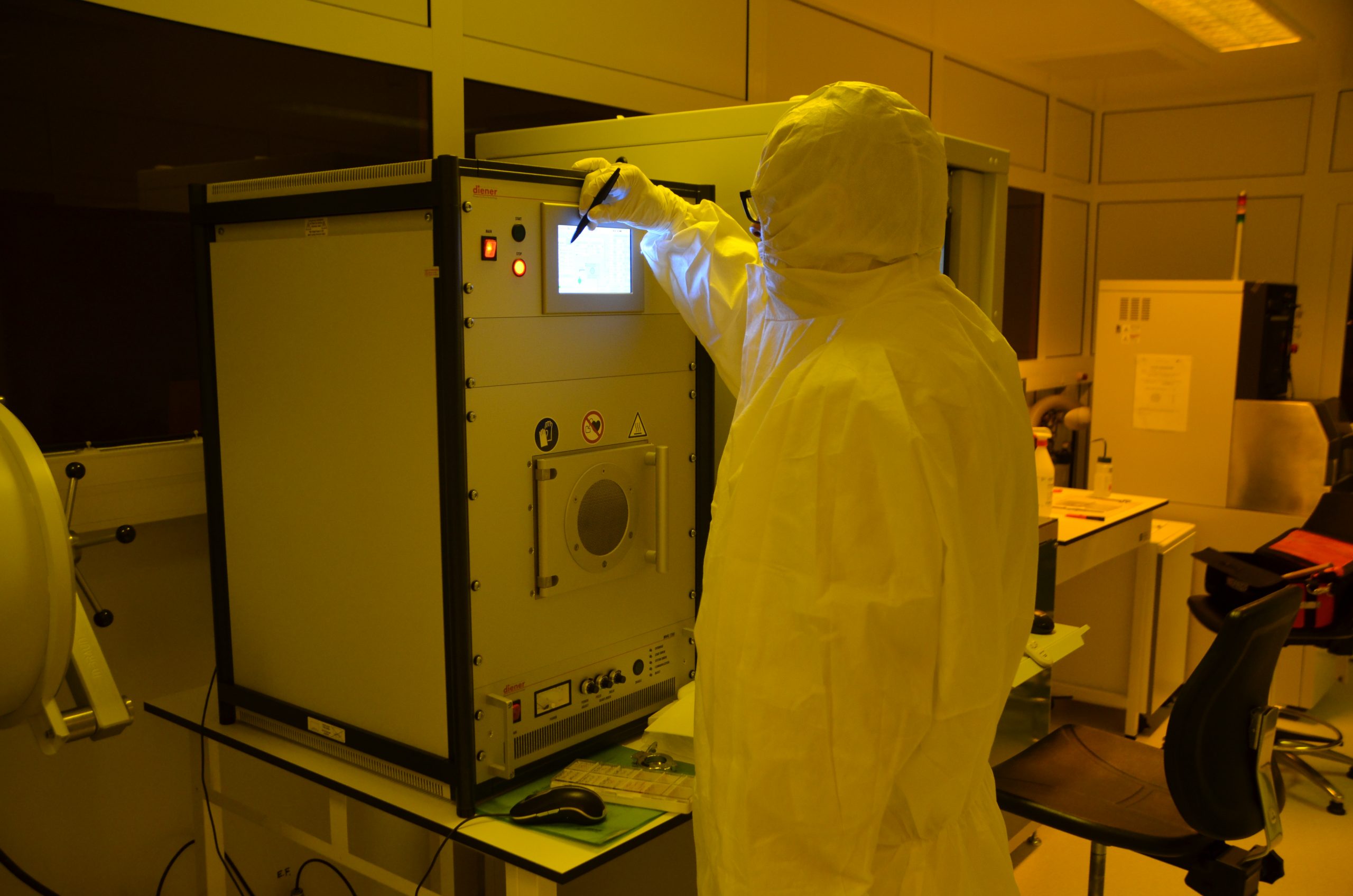
– A Diener Pico µW microwave plasma etching system
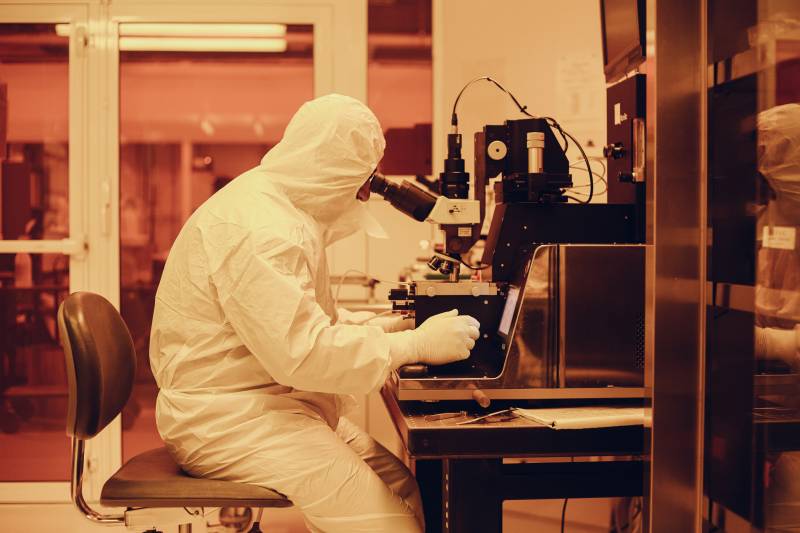
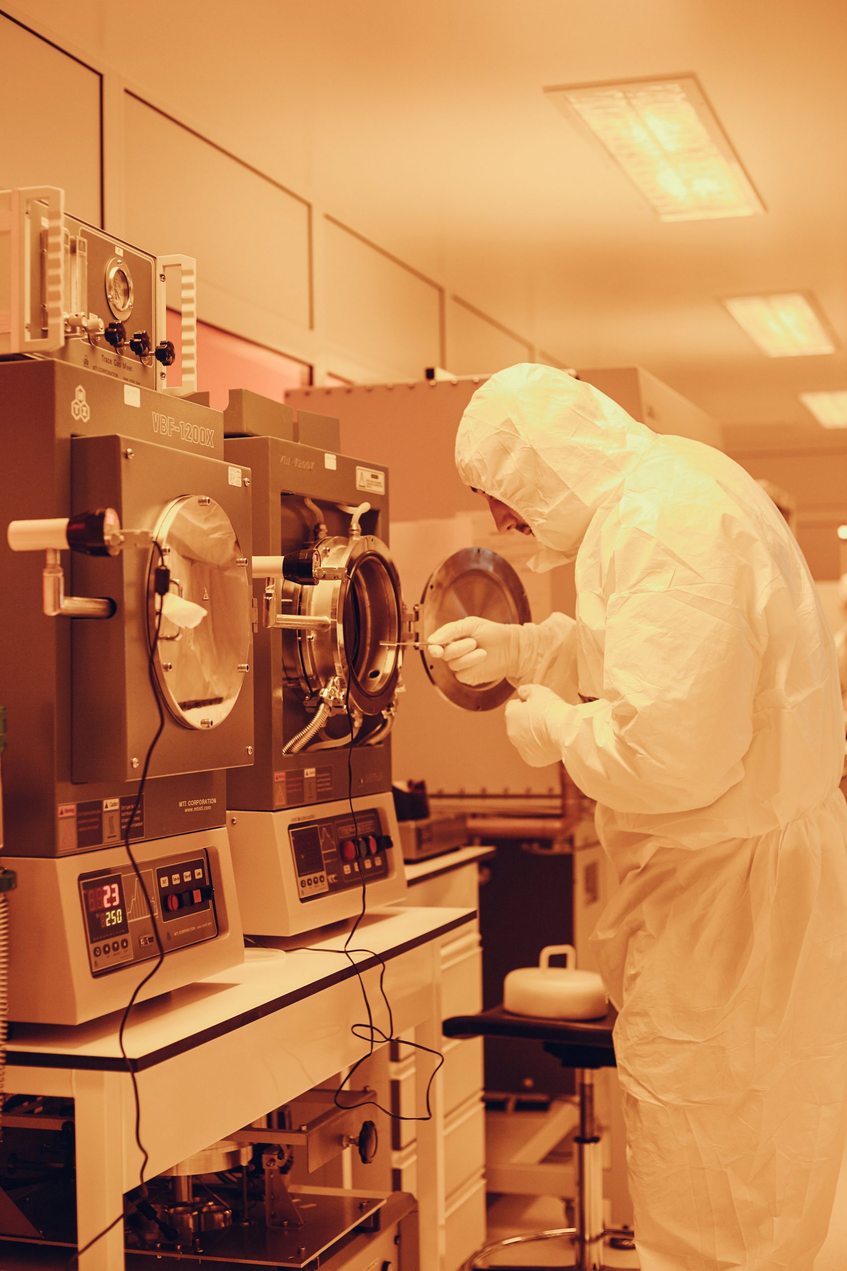
Metrology, assembly and integration of components and circuits
The range of equipment is complemented by inspection and integration tools available directly in the cleanroom. The equipment available is as follows
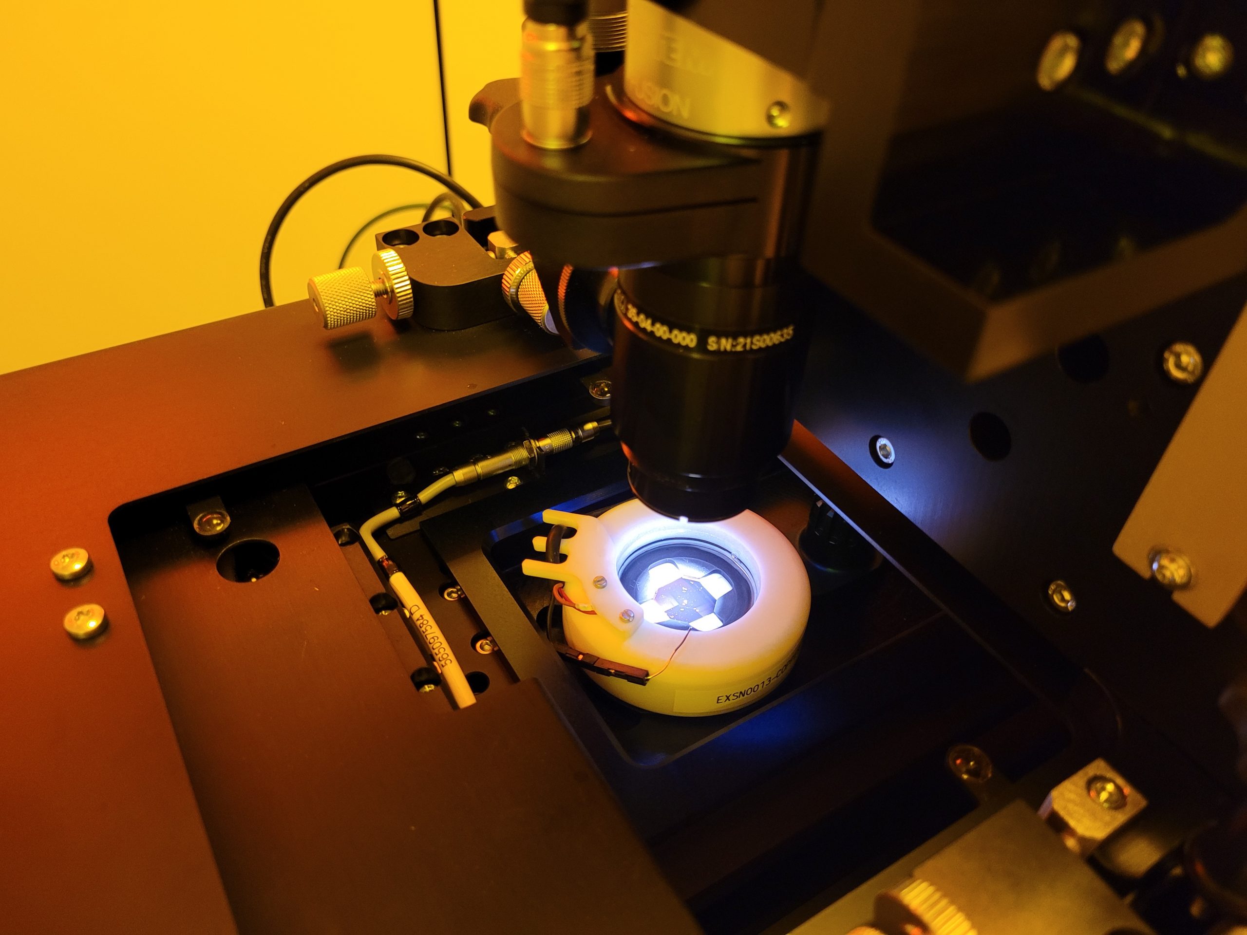
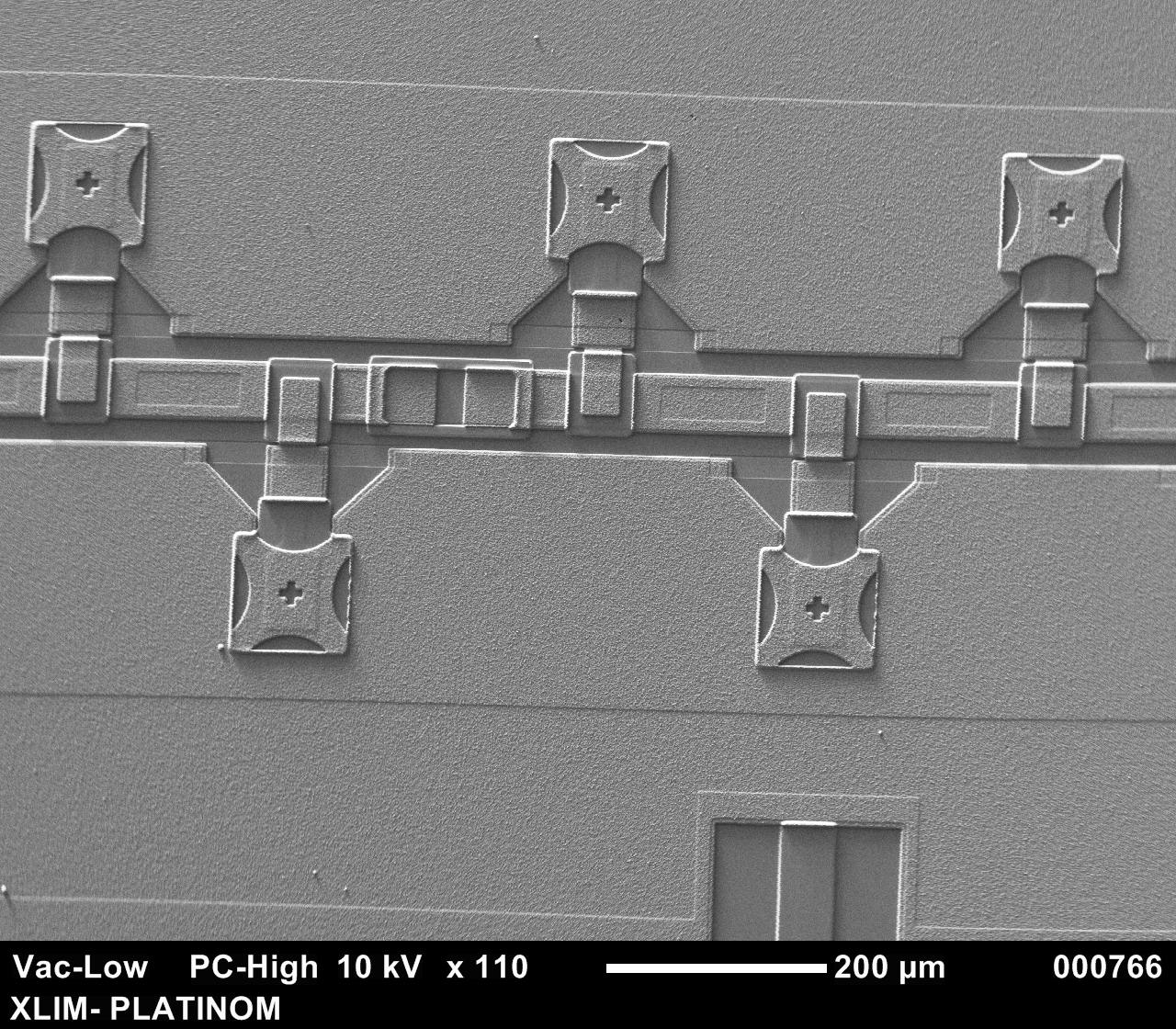
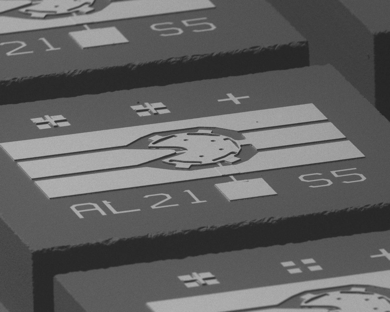
– A bench-top SEM (Nikon Jeol JCM 5000) for rapid inspection of layers of materials and patterns with a resolution of the order of a hundred nanometres,

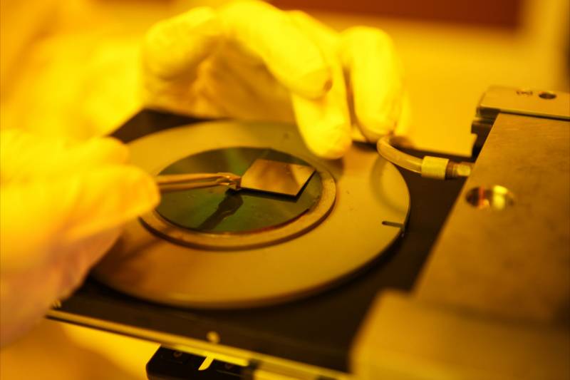
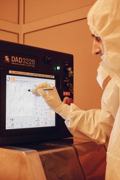
– An automatic dicing saw (Disco DAD 3220) for high-precision cutting of substrates, wafers and circuits
– A chip and component transfer system for integration using silver glue,
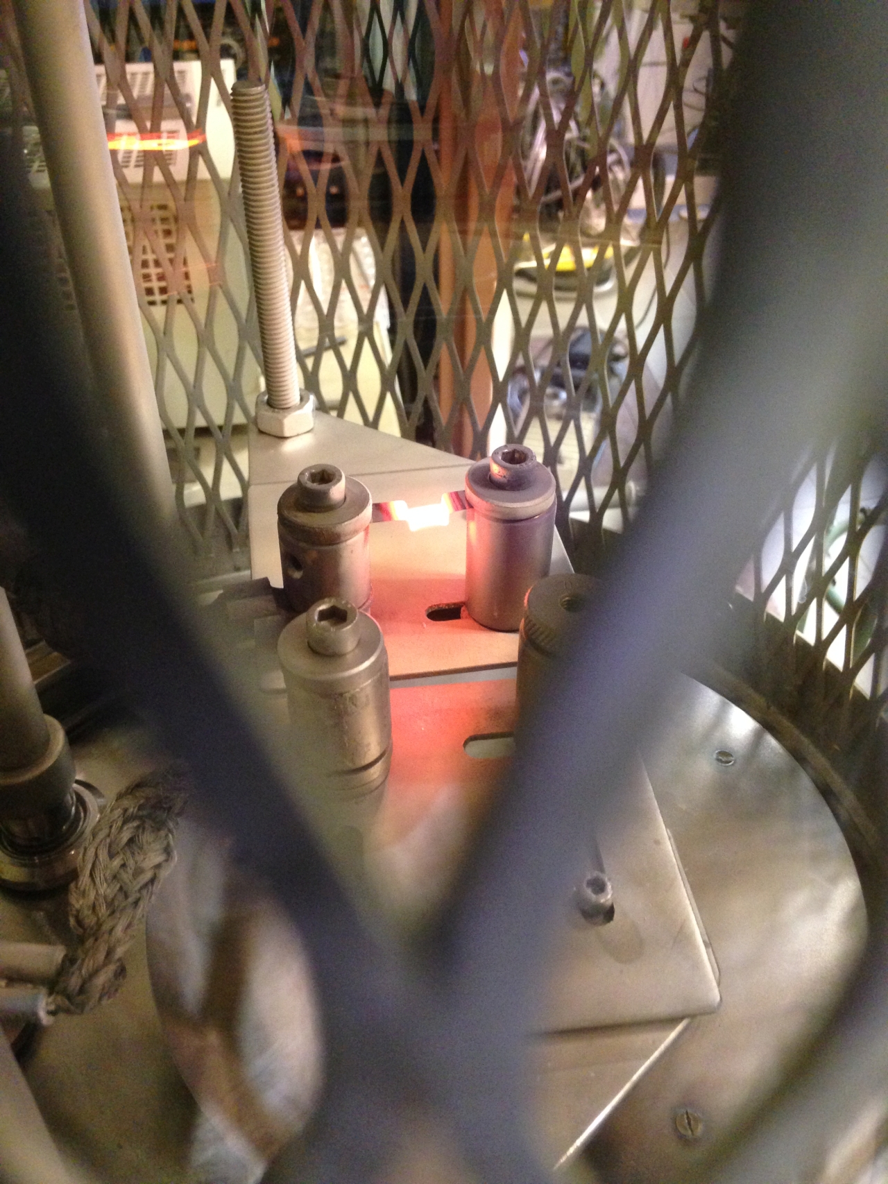
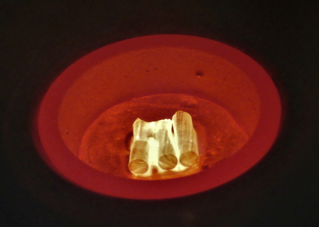
– Vacuum annealing furnaces for high-temperature annealing up to 850°C
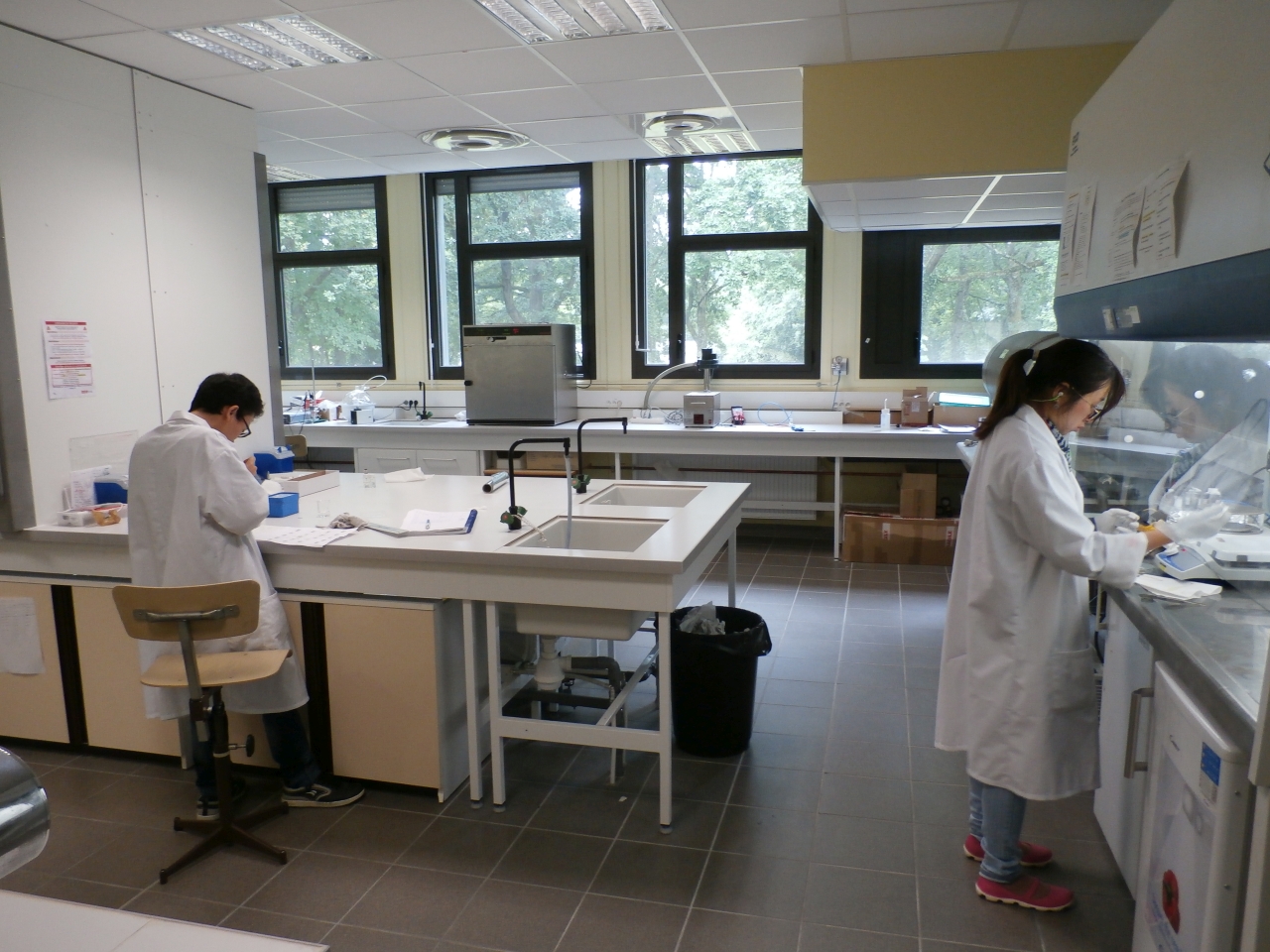
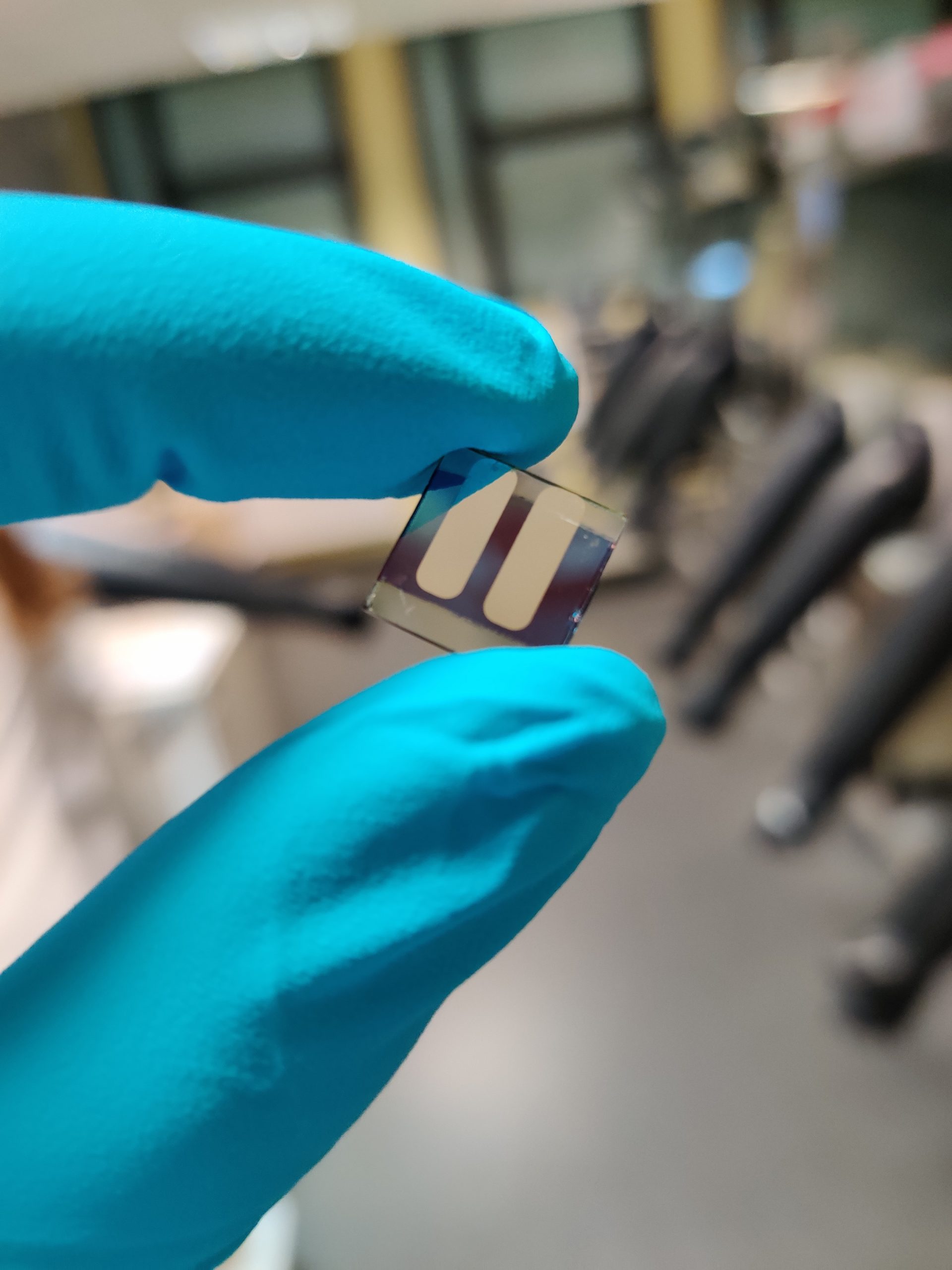
Printed electronics and optoelectronics
Wet and dry deposition processes
Wet process :
The Printed Electronics Division makes extensive use of wet thin-film deposition processes, using a number of spin coating units installed in fume cupboards in a dedicated room, or in glove boxes under an inert atmosphere. It initially enables the preparation of a variety of inks, based on molecular materials, polymers, carbon-based nano-objects (nanotubes, graphene, etc.) or semiconductors (nanocrystals). The unit is also equipped for substrate preparation (UV-ozone) and thermal annealing up to 500°C (in air and an inert atmosphere).
Physical processes:
The domain is equipped with 6 vacuum thermal evaporation systems, including 3 multi-crucible systems and 1 ion beam assisted e-beam (IBAD) system for the deposition of common electrode metals (Au, Al, Ag, etc.), inorganic semiconductor oxides (ZnO, MoO3, WO3, etc.) and low molecular weight organic semiconductors (small molecules: C60, BCP, TPBi, etc.).
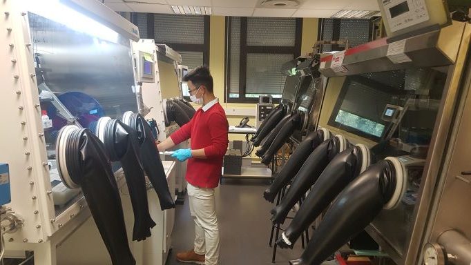
Inert atmosphere processes :
The laboratory is distinguished by its 4 gloveboxes, one of which is humidity-controlled, making it possible to separate the development of processes dedicated to organic materials from halogenated perovskite processes. They are used for wet deposition, thermal post-treatment, physical deposition ( multi-crucible thermal evaporator and ion-beam assisted electron gun deposition) and optoelectronic characterisation (current-voltage source, solar simulator).
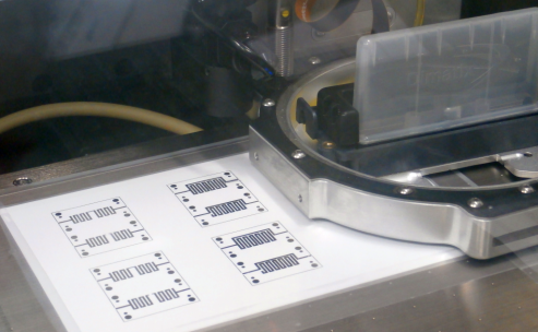
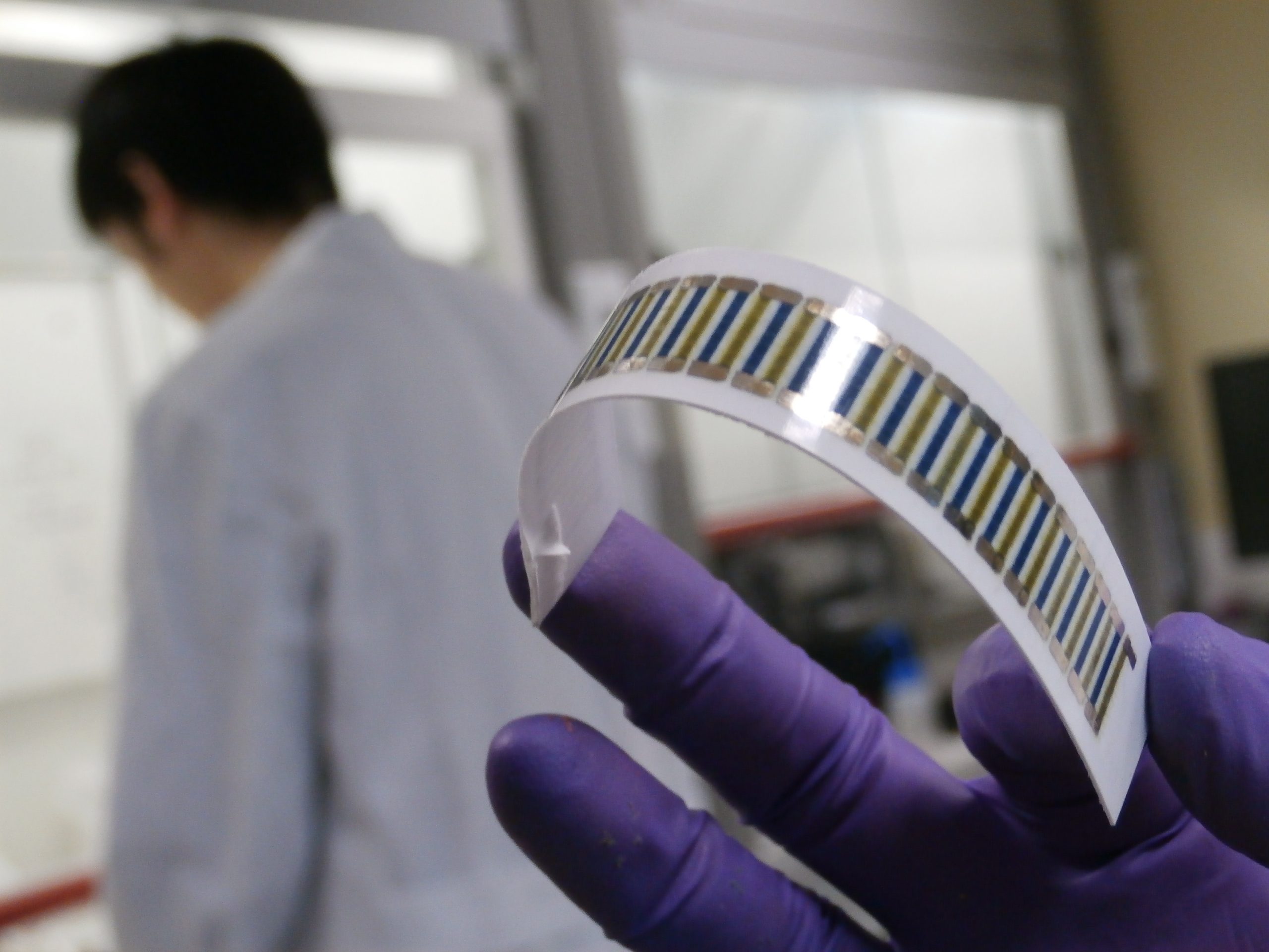
With a view to developing printable solutions, the domain is equipped with a DIMATIX printer (DMP-2831), which, coupled with rheological measurement equipment (contact angle measurement, viscosimeter), demonstrates the feasibility of printing on rigid or flexible substrates on a laboratory scale (<400 cm²).
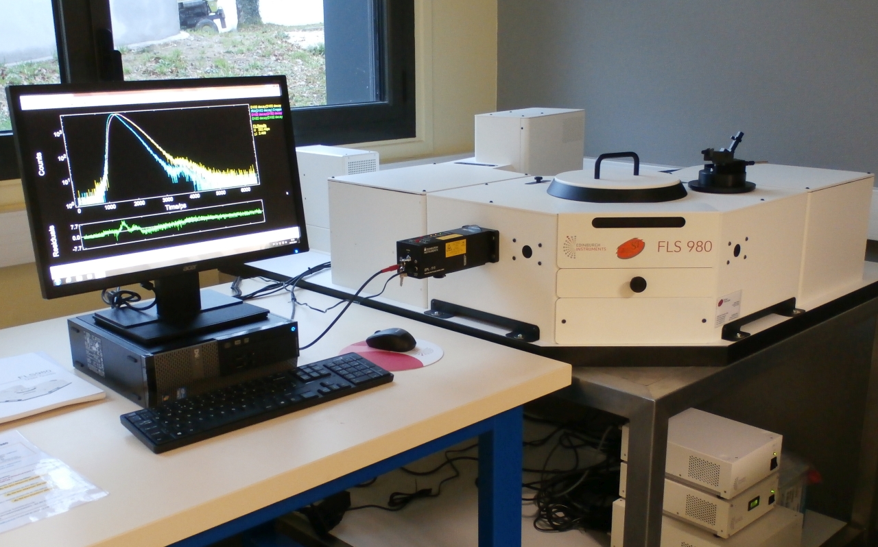
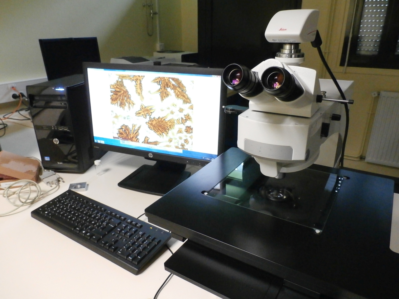
The domain allows first-level morphological characterisation in terms of roughness and topology with, in particular: – A Dektak XT mechanical profilometer, – A CSI Instruments AFM, It also enables optical characterisation of several properties of interest (reflectance, absorbance, transmittance) using a range of complementary equipment and spectrometers such as: – A LEICA DM 1200 M optical microscope, – An AGILENT Cary 300 reflectometer (integrating sphere), – A Gonio-photometer. It also has an Edinburgh Instruments fluorimeter (FLS-980), equipped for detection in the visible and infrared (up to 1400 nm), in stationary and transient mode (TRPL in TSCPC mode).
Electrical characterisation of materials and devices is offered via 4-point conductivity measurement, measurement of electrical characteristics, impedance spectroscopy (up to 120 MHz) or advanced characterisation using a semiconductor device analyser (Keithley 4200). Tests can be carried out under spikes, in an insulated rack or on a temperature-controlled stage (LINKAM). Original equipment for simultaneous measurement of electrical conductivity / thermal conductivity / Seebeck coefficient is also used to characterise thin films at liquid nitrogen temperatures of up to 200°C (TFA LINSEIS).

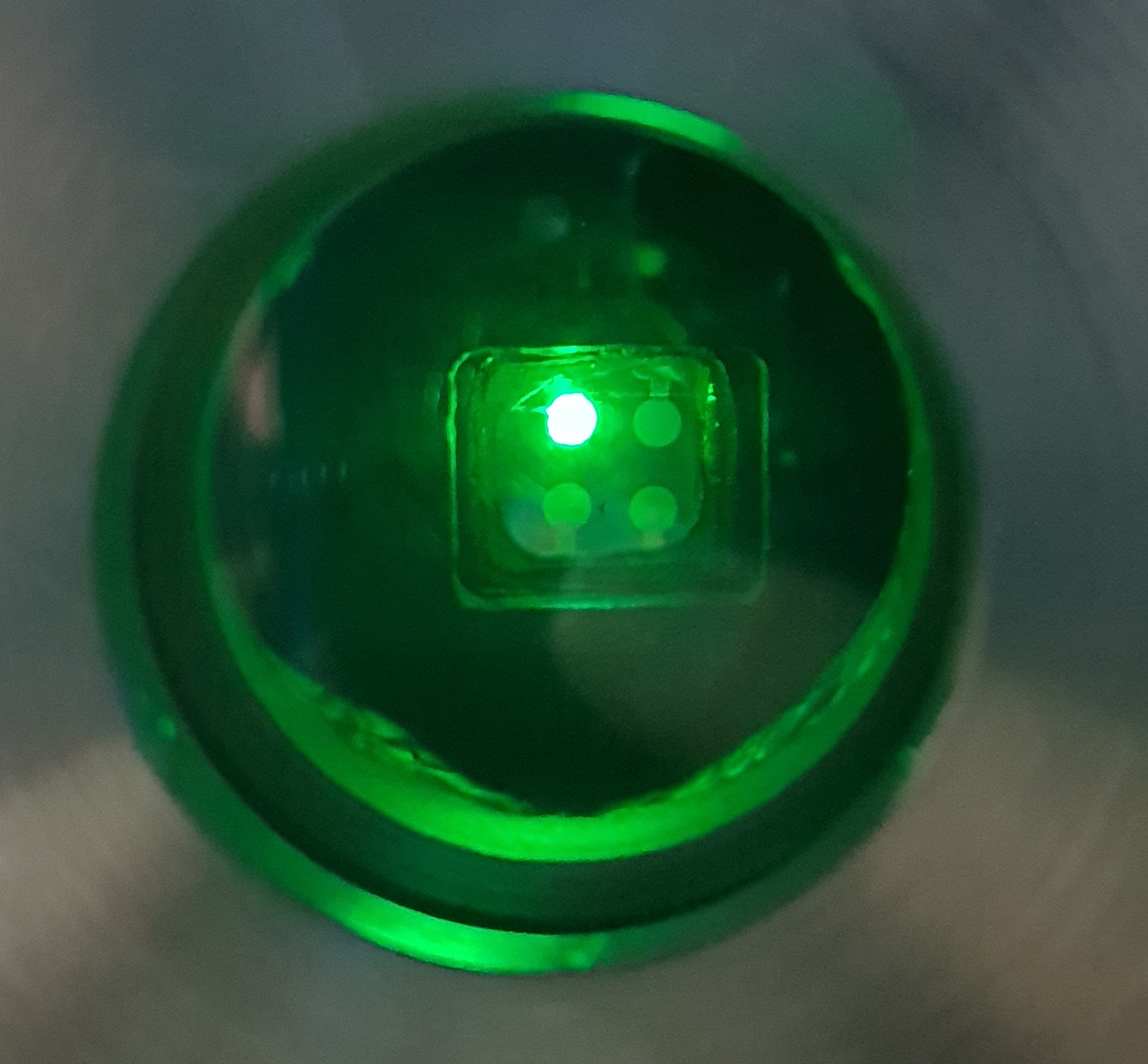
The Printed Electronics domain offers optoelectronic characterisation of a variety of devices, using conventional and/or advanced techniques: – Performance characterisation under calibrated solar simulators (AM1.5G, 100 mW/cm²) in air or in an inert atmosphere, as well as performance characterisation under indoor conditions (calibrated white LEDs, from 50 to 5000 Lux) are available for photovoltaic components, – An external quantum efficiency measurement bench (IPCE), a time-resolved photo-voltage / photo-current decay measurement bench, and a system for mapping the electrical response of PV modules (LBIC technique) are also available. In addition, the centre can characterise the performance of light-emitting diodes (LEDs) of different technologies (luminance/emission spectrum). The emission / field of view diagrams of components can also be measured, particularly for applications in the field of optical wireless communications in the visible range.